Popular Posts

Sunday 2 October 2011

Carbon Nanotubes Could Make Efficient Solar Cells


ScienceDaily — Using a carbon nanotube instead of traditional silicon, Cornell researchers have created the basic elements of a solar cell that hopefully will lead to much more efficient ways of converting light to electricity than now used in calculators and on rooftops

In a carbon nanotube-based photodiode, electrons (blue) and holes (red) - the positively charged areas where electrons used to be before becoming excited - release their excess energy to efficiently create more electron-hole pairs when light is shined on the device. (Credit: Nathan Gabor)
The researchers fabricated, tested and measured a simple solar cell called a photodiode, formed from an individual carbon nanotube. Reported online Sept. 11 in the journal Science, the researchers -- led by Paul McEuen, the Goldwin Smith Professor of Physics, and Jiwoong Park, assistant professor of chemistry and chemical biology -- describe how their device converts light to electricity in an extremely efficient process that multiplies the amount of electrical current that flows. This process could prove important for next-generation high efficiency solar cells, the researchers say.
"We are not only looking at a new material, but we actually put it into an application -- a true solar cell device," said first author Nathan Gabor, a graduate student in McEuen's lab.
The researchers used a single-walled carbon nanotube, which is essentially a rolled-up sheet of graphene, to create their solar cell. About the size of a DNA molecule, the nanotube was wired between two electrical contacts and close to two electrical gates, one negatively and one positively charged. Their work was inspired in part by previous research in which scientists created a diode, which is a simple transistor that allows current to flow in only one direction, using a single-walled nanotube. The Cornell team wanted to see what would happen if they built something similar, but this time shined light on it.
Shining lasers of different colors onto different areas of the nanotube, they found that higher levels of photon energy had a multiplying effect on how much electrical current was produced.
Further study revealed that the narrow, cylindrical structure of the carbon nanotube caused the electrons to be neatly squeezed through one by one. The electrons moving through the nanotube became excited and created new electrons that continued to flow. The nanotube, they discovered, may be a nearly ideal photovoltaic cell because it allowed electrons to create more electrons by utilizing the spare energy from the light.
This is unlike today's solar cells, in which extra energy is lost in the form of heat, and the cells require constant external cooling.
Though they have made a device, scaling it up to be inexpensive and reliable would be a serious challenge for engineers, Gabor said.
"What we've observed is that the physics is there," he said.
The research was supported by Cornell's Center for Nanoscale Systems and the Cornell NanoScale Science and Technology Facility, both National Science Foundation facilities, as well as the Microelectronics Advanced Research Corporation Focused Research Center on Materials, Structures and Devices. Research collaborators also included Zhaohui Zhong, of the University of Michigan, and Ken Bosnick, of the National Institute for Nanotechnology at University of Alberta
Story Source:ScienceDaily
The above story is reprinted (with editorial adaptations by ScienceDaily staff) from materials provided by Cornell University. The original article was written by Anne Ju

Sunday 1 May 2011

Graphene Holds Great Promise for Microelectronics

Graphene – a sheet of carbon atoms linked in a hexagonal, chicken wire structure – holds great promise for microelectronics. Only one atom thick and highly conductive, graphene may one day replace conventional silicon microchips, making devices smaller, faster and more energy-efficient.

In addition to potential applications in integrated circuits, solar cells, miniaturized bio devices and gas molecule sensors, the material has attracted the attention of physicists for its unique properties in conducting electricity on an atomic level.

Placed on boron nitride, graphene shows much smaller electric charge fluctuations, shown in red and blue (left) than when mounted on a silicon oxide wafer (right).

Otherwise known as pencil "lead," graphene has very little resistance and allows electrons to behave as massless particles like photons, or light particles, while traveling through the hexagonal grid at very high speeds.
The study of the physical properties and potential applications of graphene, however, has suffered from a lack of suitable carrier materials that can support a flat graphene layer while not interfering with its electrical properties.
Researchers in the University of Arizona's physics department along with collaborators from the Massachusetts Institute of Technology and the National Materials Science Institute in Japan have now taken an important step forward toward overcoming those obstacles.
They found that by placing the graphene layer on a material almost identical in structure, instead of the commonly used silicon oxide found in microchips, they could significantly improve its electronic properties.
Substituting silicon wafers with boron nitride, a graphene-like structure consisting of boron and nitrogen atoms in place of the carbon atoms, the group was the first to measure the topography and electrical properties of the resulting smooth graphene layer with atomic resolution.
The results are published in the advance online publication of Nature Materials.
"Structurally, boron nitride is basically the same as graphene, but electronically, it's completely different," said Brian LeRoy, an assistant professor of physics and senior author of the study. "Graphene is a conductor, boron nitride is an insulator."
"We want our graphene to sit on something insulating, because we are interested in studying the properties of the graphene alone. For example, if you want to measure its resistance, and you put it on metal, you're just going to measure the resistance of the metal because it's going to conduct better than the graphene."
Unlike silicon, which is traditionally used in electronics applications, graphene is a single sheet of atoms, making it a promising candidate in the quest for ever smaller electronic devices. Think going from a paperback to a credit card.
"It's as small as you can shrink it down," LeRoy said. "It's a single layer, you'll never get half a layer or something like that. You could say graphene is the ultimate in making it small, yet it 's still a good conductor."
Stacked upon each other, 3 million sheets of graphene would amount to only 1 millimeter. The thinnest material on Earth, graphene brought the 2010 Nobel Prize to Andre Geim and Konstantin Novoselov, who were able to demonstrate its exceptional properties with relation to quantum physics.
"Using a scanning tunneling microscope, we can look at atoms and study them," he added. "When we put graphene on silicon oxide and look at the atoms, we see bumps that are about a nanometer in height."
While a nanometer – a billionth of a meter – may not sound like much, to an electron whizzing along in a grid of atoms, it's quite a bump in the road.
"It's basically like a piece of paper that has little crinkles in it," LeRoy explains. "But if you put the paper, in this case the graphene, on boron nitride, it's much flatter. It smooths out the bumps by an order of magnitude."
LeRoy admits the second effect achieved by his research team is a bit harder to explain.
"When you have graphene sitting on silicon oxide, there are trapped electric charges inside the silicon oxide in some places, and these induce some charge in the overlying graphene. You get quite a bit of variation in the density of electrons. If graphene sits on boron nitride, the variation is two orders of magnitude less."
In his lab, LeRoy demonstrates the first – and surprisingly low-tech – step in characterizing the graphene samples: He places a tiny flake of graphite – the stuff that makes up pencil "lead" – on sticky tape, folds it back on itself and peels it apart again, in a process reminiscent of a Rorschach Test.
"You fold this in half," he explained, "and again, and again, until it gets thin. Graphene wants to peel off into these layers, because the bonds between the atoms in the horizontal layer are strong, but weak between atoms belonging to different layers. When you put this under an optical microscope, there will be regions with one, two, three, four or more layers. Then you just search for single-layer ones using the microscope."
"It's hard to find the sample because it's very, very small," said Jiamin Xue, a doctoral student in LeRoy's lab and the paper's leading author. "Once we find it, we put it between two gold electrodes so we can measure the conductance."
To measure the topography of the graphene surface, the team uses a scanning tunneling microscope, which has an ultrafine tip that can be moved around.
"We move the tip very close to the graphene, until electrons start tunneling to it," Xue explained. "That's how we can see the surface. If there is a bump, the tip moves up a bit."
For the spectroscopic measurement, Xue holds the tip at a fixed distance above the sample. He then changes the voltage and measures how much current flows as a function of that voltage and any given point across the sample. This allows him to map out different energy levels across the sample.
"You want as thin an insulator as possible," LeRoy added. "The initial idea was to pick something flat but insulating. Because boron nitride essentially has the same structure as graphene, you can peel it into layers in the same way. Therefore, we use a metal as a base, put a thin layer of boron nitride on it and then graphene on top."
Source: http://www.arizona.edu/

Nanotechnology-based Multi-time Programmable Memory for Mobile Communications Platforms

Kilopass Technology recently launched Itera, an integrated multi-time programmable (MTP) NVM in 40nm, at the Linley Tech Mobile Conference held at the DoubleTree Hotel in San Jose, California.

Itera will enable SoC designers to reduce costs and enhance integration by replacing outside serial EEPROM and NOR flash in high-volume portable and consumer products. It is used in standard CMOS and does not need further processing or wafer process adders, and offers up to 1Mb storage capacity and 1024 cycles of re-programmability in time stamp, key retrieval, firmware updates, and trimming modulations.
The device will enhance performance over time and lower costs and product size. It can store information that needs to be retrieved repeatedly or altered, such as in tablets and multiple portable products. It can support SoCs for Bluetooth, 802.11, and wireless communications standards that help these devices to stay connected. It can store information for editing analog parts changing constantly. It is suitable for low frequency information sorting.
Its interface is an Open Core Protocol (OCP) that makes for easy integration at the front-end. Its contents can be viewed and executed in place (XIP), and do not need to be shadowed.
Source: http://www.kilopass.com

Eulitha Nanoimprint Templates


Eulitha Nanoimprint Templates
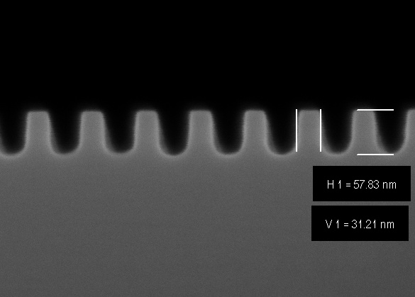
Eulitha's nanoimprint templates are manufactured with electron beam or its unique EUV lithography technology. Standard templates include 35 nm half-pitch linear gratings and 53 nm half-pitch dot arrays, both of which are made with exceptional quality thanks to the EUV exposure capability. Custom made templates are made according to customer specifications with the most suitable technology choice: EUV technology enables production of high-resolution periodic structures (sub-100nm) over large areas whereas e-beam is used for making arbitrary patterns.
Applications of Eulitha's templates include process development and verification, nano-optics, SERS substrates, patterned magnetic media, microscope calibration, nano-electronics and templated self-assembly. Contact us with your needs for expert advice from our world-renowned scientific staff.
Key features:
  • Resolution down to 20 nm
  • Anti-adhesion coating (optional)
  • Quick turn around time of 4-6 weeks
  • Area/resolution combinations (e.g. 35 nm over 1cm2)

Thursday 28 April 2011

Reflective Gold Nano-particles to Track Colon Cancer Cells

A team led by Sanjiv Gambhir of Stanford University is endeavoring to create molecular signals, or nano-particles that will help physicists view pre-cancerous polyps not visible to the naked eye. The team has been analyzing a nanoparticle used in anti-counterfeiting.


Stnford University says the use of gold nanoparticles during a colonoscopy could help doctors detect small, easily overlooked polyps.

Gold-silica nanoparticles are incorporated into security documents such as paper money to confirm their genuineness. The particles diffuse light in a particular manner, helping discern real currency from forged ones. The team added a surface layer to these nano-particles to enable them to bind to cancer cells.
Peptides and proteins were applied to the nano-particles to help identify cancer cells in the initial stages. The nano-particles bind easily to cancer cells.
A patient suffering from colon cancer would first drink a liquid having multitude of nano-particles. As they descend to the bowel, they bind to the tumor cells on the way. The procedure helps the physician to view the bright nano-particles attached to the cancer cells
Gambhir says that government approval for the technique could be received by end 2012. The research paper has recently appeared in the journal, Science Translational Medicine.
Source: http://www.stanford.edu

SiTime has recently declared the availability of its portfolio of MEMS oscillators to be used in Tablet PCs and E-Book Readers.

 The solutions, based on the company’s SiT8003 Low Power MEMS Oscillator platform, deliver clocking for every functional block in the Tablet PC and E-Book Reader. It offers resilience to shock and vibration, and enhances aesthetics and lifespan of the electronic devices it is being incorporated into.
Piyush Sevalia, vice president of marketing at SiTime said that tablet PCs and E-Book Readers are expected to be exported more than 200 million units over the next four years.
The low-power programmable oscillator can be used to develop multiple devices within a Tablet PC and E-Book Reader. It consumes 3.5mA in active mode and less than 5µA in standby mode, offering ±25PPM frequency stability over -20 to 70ºC and comes in a nano-sized, 2.5x2.0mm package. It offers configurable rise and fall times without needing further investment. The various clocks can be controlled to reduce system EMI and meet environmental compliance cost-effectively and without changing the design.
Source: http://www.sitime.com